General Description
This document provides information on the function and use of the RTQ6050 evaluation board (EVB), as well as instructions for operating and modifying the board and circuit to meet individual requirements. Additionally, it includes details on the schematic diagram, bill of materials, and evaluation board layout.
Performance Specification Summary
Summary of the RTQ6050GF Evaluation Board performance specificiaiton is provided in Table 1. The ambient temperature is 25°C.
Table 1. RTQ6050GF Evaluation Board Performance Specification Summary
|
Specification
|
Test Conditions
|
Min
|
Typ
|
Max
|
Unit
|
|
Default Input Voltage
|
Default = 12V
|
2
|
--
|
80
|
V
|
|
Supply Voltage
|
Default = 12V
|
2.9
|
--
|
18
|
V
|
|
Sensing Current
|
|
--
|
0.5
|
--
|
A
|
|
Output Voltage
|
|
--
|
5
|
--
|
V
|
|
Gain
|
|
--
|
20
|
--
|
V/V
|
|
Gain Error
|
|
--
|
--
|
±2
|
%
|
|
Offset Voltage, RTI
|
|
--
|
±0.5
|
±2.5
|
mV
|
|
Quiescent Current
|
VOUT = 2V, TA = -40oC to 125oC
|
--
|
--
|
1200
|
μA
|
Power-up & Measurement Procedure
Suggestion Required Equipments
- RTQ6050GF Evaluation Board
- DC Power Supply (Chroma, 62006P-100-25)
- Electronic load capable of 6A
- Function Generator
- DC Meter
- Oscilloscope
Quick Start Procedures
1. Apply VCC = 12V input power supply (2.9V < VCC < 18V) to VCC and GND terminals.
2. Apply VIN+ = 12V input power supply (2V < VIN+ < 80V) to VIN+ and GND terminals.
3. The default sense resistance is 100mΩ.
4. Connect an external load to VIN- and GND terminals, and keep loading current = 0.5A.
5. Measure the sense voltage (approximately 50mV) between VIN+ and VIN-.
6. Measure the output voltage (approximately 1V) between VOUT and GND.
Comparator Input, R3, and R4
The RTQ6050 devices incorporate an open-drain comparator. This comparator typically has 1.3μs (typical) response time. The output of the comparator latches and is reset through the #RESET pin. The negative terminal is connected to a 0.6V internal reference, and the positive comparator input is connected to the CMPI pin of the device. Adjust R3 and R4 (show in EVB schematic) to set the comparator trip point for the intended application, where CMPI = (OUT × R4) / (R3 + R4) = 0.6V.
Detailed Description of Hardware
Headers Description and Placement
Carefully inspect all the components used in the EVB according to the following Bill of Materials table, and then make sure all the components are undamaged and correctly installed. If there is any missing or damaged component, which may occur during transportation, please contact our distributors or e-mail us at evb_service@richtek.com.
Test Points
The EVB is provided with the test points and pin names listed in the table below.
|
Test point
|
Function
|
|
VCC
|
Power input test point.
|
|
OUT
|
Output Voltage test point.
|
|
CMPI
|
Comparator input test point.
|
|
GND
|
Ground.
|
|
#RESET
|
Reset input pin.
|
|
CMPO
|
Open-drain comparator output.
|
|
VIN-
|
Negative current-sensing input.
|
|
VIN+
|
Positive current-sensing input.
|
|
JP1
|
VCC to ground test point.
|
|
JP2
|
RESET jumper. Connect RESET to ground or pull high to VCC.
|
|
SW1
|
RESET control switch. Connect RESET to ground or pull high to VCC.
|
Bill of Materials
|
Reference
|
Count
|
Part Number
|
Value
|
Description
|
Package
|
Manufacturer
|
|
C1, C2, C5
|
3
|
GRM188R71H104KA93D
|
0.1µF/25V/X7R/0603
|
Capacitor, Ceramic
|
0603
|
MURATA
|
|
R1, R2
|
2
|
RTT05000JTP
|
0/0805
|
Resistor
|
0805
|
RALEC
|
|
R3, R4
|
2
|
RTT031001FTP
|
1k/0603
|
Resistor
|
0603
|
RALEC
|
|
R5
|
1
|
WR06X1003FTL
|
100k/0603
|
Resistor
|
0603
|
WALSIN
|
|
R6
|
1
|
RTT034701FTP
|
4.7k/0603
|
Resistor
|
0603
|
RALEC
|
|
RSEN1
|
1
|
RTT25R100FTE
|
0.1
|
Resistor
|
2512
|
RALEC
|
|
U1
|
1
|
RTQ6052GF
|
RTQ6052GF
|
CSOP
|
MSOP-8
|
RICHTEK
|
Typical Applications
EVB Schematic Diagram
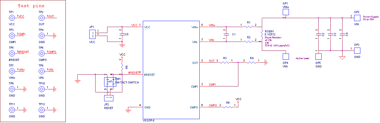
Note:
1. Do not hot-plug input voltage and supply voltage on the boar. If hot-plugging is required, add ~100µF electrolytic capacitor at the input.
2. All the stated input and output capacitor values are the effective capacitances, including any de-rating effect, like a DC Bias. The stability of the converter may be impacted when using small size MLCC output capacitors, which may have much lower capacitance at the application DC output voltage than the rated value.
Measurement Results
|
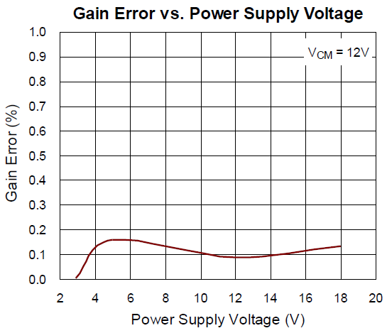
Gain Error with Power Supply (VS) Measurement
|
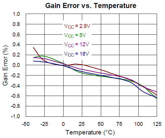
Gain Error with Temperature Measurement
|
|
|
|
|
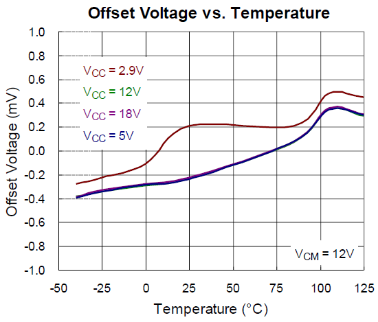
Offset Voltage with Temperature Measurement
|
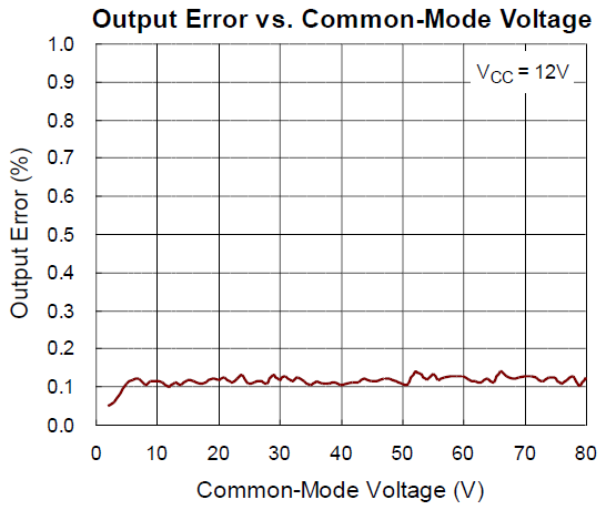
Output Error with Common-Mode Measurement
|
|
|
|
|
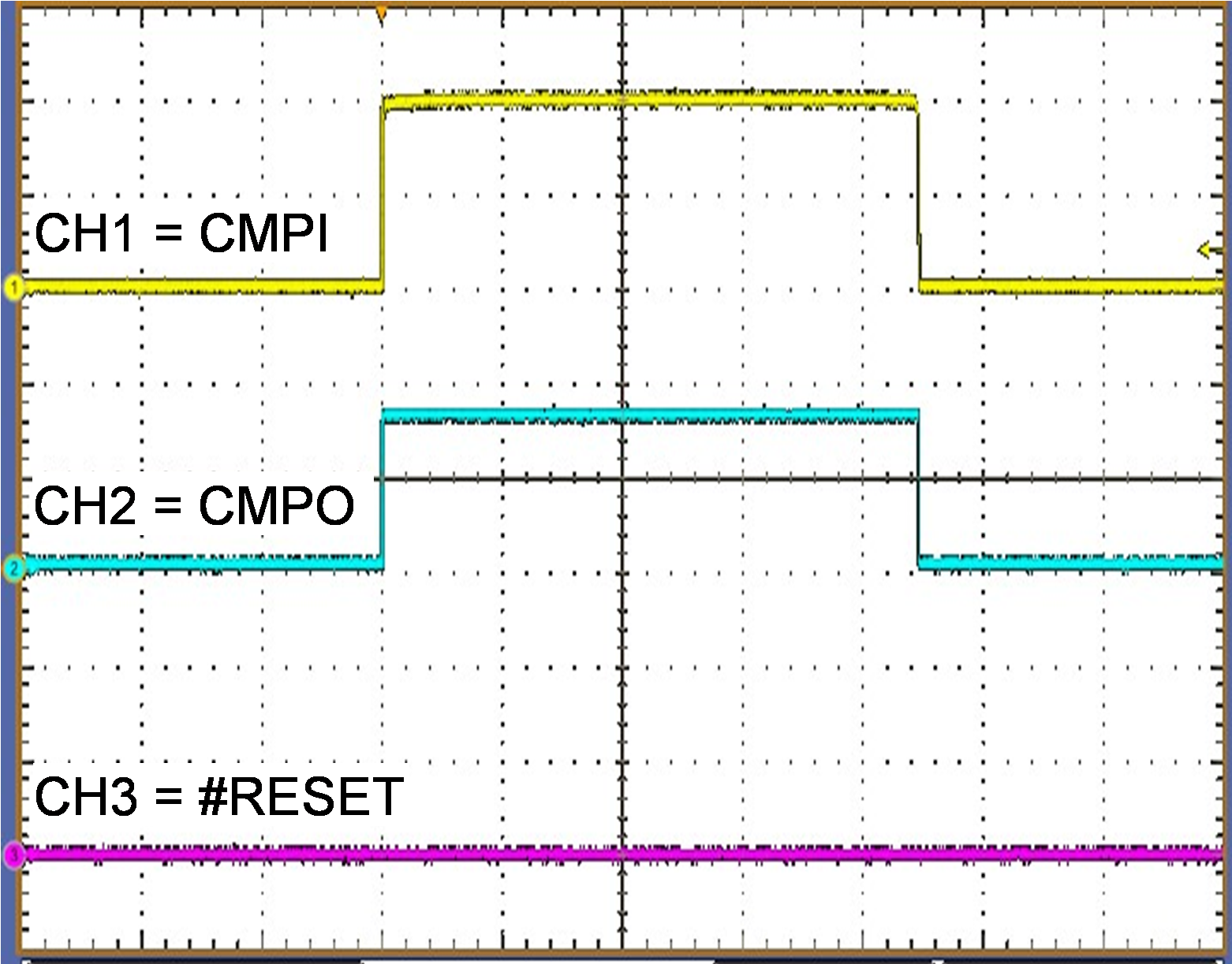
#RESET signal = Low, CMPO is dominated by CMPI and 0.6V
|
|
|
|
|
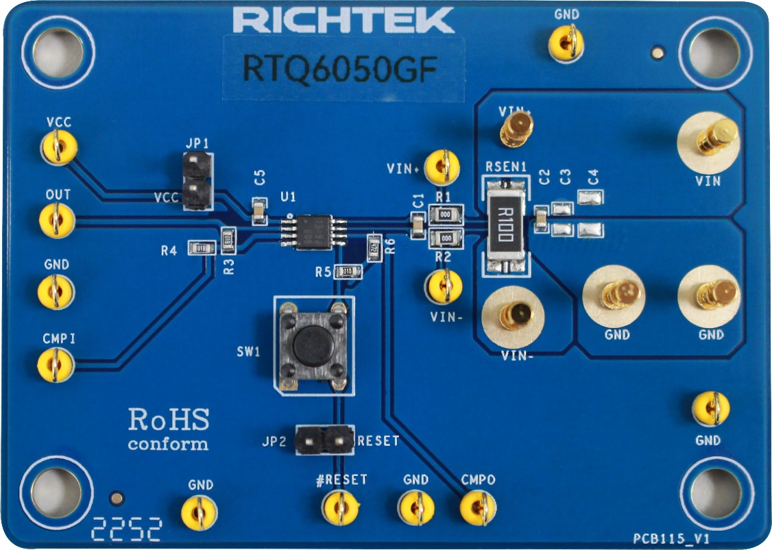
Evaluation Board Layout
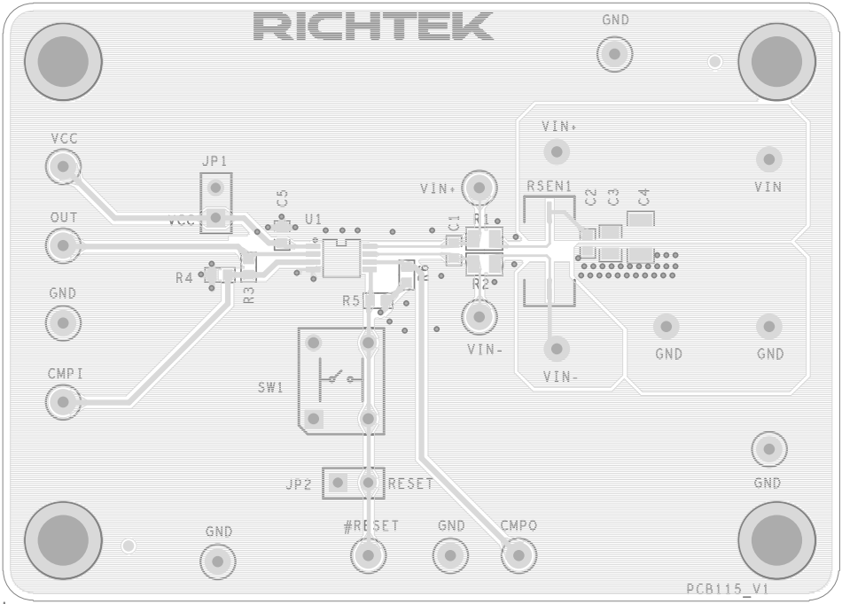
Figure 1. Top View
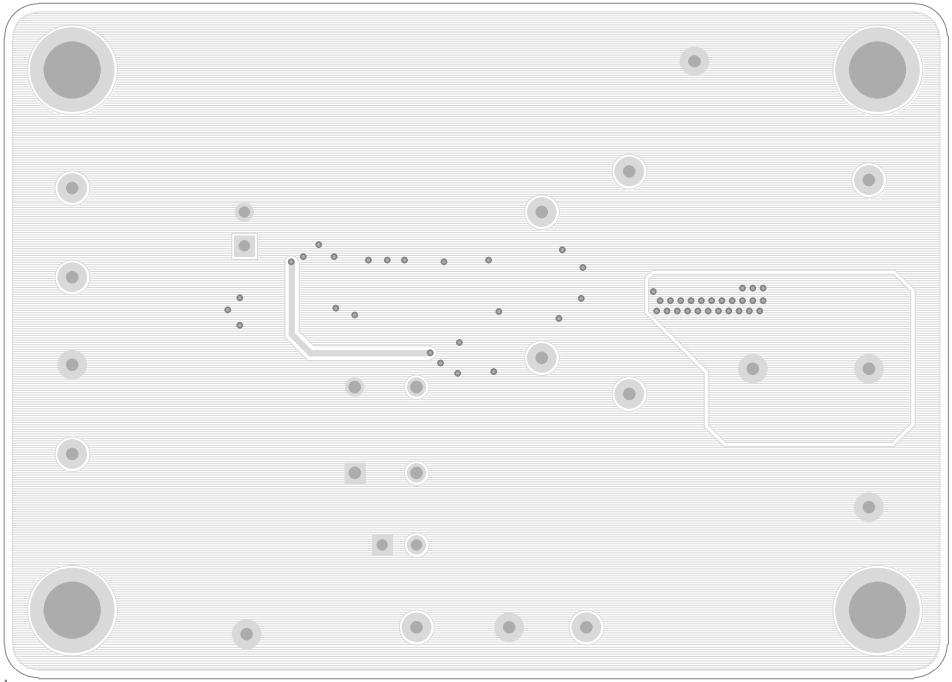
Figure 2. Bottom View